SMD Stencils / Precision Stencils

Laser-cut precision stencils and SMD stencils from KMLT®

Laser-cut precision stencils such as SMD stencils are the standard for the precise application of solder and printing pastes, adhesives and other materials to rigid or flexible printed circuit boards as well as to surfaces such as silicon wafers (wafer bumping), glass or ceramic substrates (LTCC). These stencils enable precise placement and volume definition, which is crucial for the subsequent automated assembly of electronic components such as microchips, SMD components, contact elements and other semiconductor components. This technology is also used in flip-chip assembly.

Our precision stencils are available in all standard formats and for all quick-release frames. For particularly demanding applications, we also offer electropolishing in combination with nanocoating to further improve the performance and durability of the stencils.

Advantages of our precision stencils:

  • Highest precision: laser-cut stencils guarantee exact material application.
  • Versatility: Suitable for rigid and flexible PCBs and various substrates.
  • Automated assembly: Perfect preparation for the placement and fusion of electronic components.
  • Advanced options: Electropolishing and nanocoating for demanding applications.

Opt for precision templates from KMLT® and benefit from our expertise and advanced technologies in laser cutting technology.
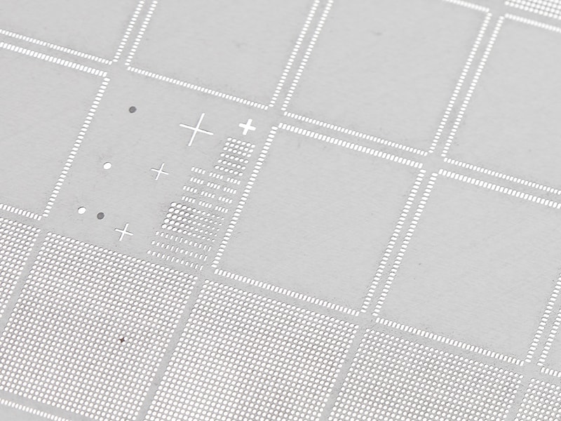
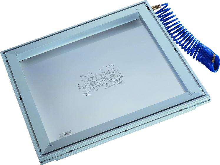
SMD stencils

Foto
  • Laser-cut SMD metal stencils for the industrial production of electronic assemblies

    Laser-cut SMD metal stencils are essential in the industrial production of electronic assemblies. They are used to precisely apply solder pastes or adhesives to printed circuit boards, which enables subsequent assembly with SMD components.

  • Frameless stencils with perforation for quick clamping systems

    Depending on the customer’s technical requirements, these stencils are typically manufactured as frameless stainless steel foil with perforations for a quick-clamping system. In addition to traditional systems, we produce high-precision stencils for VectorGuard™ quick-clamping systems, as well as special versions with optional electropolishing or nano-coating for optimized solder paste release.

  • Data processing

    The data processing of SMD stencils includes several important steps to ensure that the stencils can be used accurately and efficiently for solder paste printing. Here are some examples that we take into account during data processing:

    • Layout analysis: reviewing the pad layout, examining for optimization opportunities in pad shape and pad arrangement
    • Design rules: Checking for compliance with basic design rules such as the area ratio (area ratio) and aspect ratio (pad width – stencil thickness ratio) for optimum material application and avoidance of printing errors such as bridging or tombstone effects
    • Multiple duplicate creation: layout duplications and insertion of fiducials
    • Material recommendation and stencil thickness: Selection of the correct sheet thickness according to the specific requirements of the components and the layout – recommendations for special materials if necessary
  • Quality inspection of SMD stencils

    Before delivery, each SMD stencil is subjected to an optical quality check on a scanner. This enables us to guarantee maximum precision and quality in order to meet the requirements of modern electronics production.

SMD stencils in the VectorGuard™ format

VectorGuard™ stencils: Stainless steel 1.4301 and FineGrain material for maximum precision

In addition to stencil sheets made from 1.4301 stainless steel, we now also offer VectorGuard™ stencils made from the innovative FineGrain material. This stainless steel sheet with a particularly fine grain is a cost-effective alternative to nickel and enables smoother inner pad walls during laser cutting. The aim is to further improve the release behavior of pastes.

Advantages of FineGrain materials

  • Fine grains: FineGrain material provides a smooth and uniform surface that is ideal for precise printing.
  • Cost-effective alternative: FineGrain stainless steel is an economical solution compared to nickel, without compromising on quality.
  • Improved paste release: The smoother inner pad walls ensure optimized paste release and increase transfer efficiency.
  • Ideal for high-density applications: Particularly suitable for demanding applications that require maximum precision and reliability.

Applications

VectorGuard™ stencils made of FineGrain material are particularly interesting for high-density applications in electronics production where maximum precision and efficiency are required.

License-free perforations for quick-clamping systems

Electropolishing of SMD stencils

  • Electropolishing to optimize the inner pad edges

    During electropolishing, the surface of an anodized workpiece is abraded under the influence of direct current and electrolyte, particularly on tips and edges. This process leads to a leveling of the micro-roughness and the finest deburring, while passivity and corrosion resistance are retained.

  • KMLT® recommends electropolishing for SMD stencils

    For demanding SMD stencils, KMLT® also recommends electropolishing for surface optimization. Electropolishing minimizes the roughness within the pad walls, which significantly improves the release of the solder paste.

  • Advantages of electropolishing

    • Extremely smooth and burr-free surfaces: Electropolished stencils can be cleaned better at significantly increased intervals.
    • Improved solder paste release: Minimized roughness within the pad walls optimizes the production process.

    Further information on Electropolishing can be found under surface treatment.

Nano-coating for precision stencils

  • Optimization by Aculon® NanoClear® layer

    For precision stencils, it is possible to seal the surface with an Aculon® NanoClear® coating. This nano-coating ensures that solder paste residues adhere less strongly to the pads or no longer adhere at all. This makes the stencil even easier and quicker to clean.

  • Advantages of nanocoating

    • Easy cleaning: The optimized stencil is much easier to clean.
    • Durability: This type of treatment is usually sufficient for several tens of thousands of printing processes.
    • Repeatability: The nano-coating can be repeated at any time if required.

    Take advantage of KMLT® nano-coating to maximize the efficiency and longevity of your precision stencils.

FAQ: SMD and Precision Stencils from KMLT®

What is an SMD stencil, and what is it used for?

SMD stencils serve as precise mechanical masks in electronics manufacturing. They ensure that solder paste or adhesive is applied accurately, consistently, and without errors to the contact areas of a printed circuit board. This optimally prepares the printed circuit board for subsequent automated component placement.

What are the typical thicknesses and dimensions of the stencils?

The thickness of the stencil determines the amount of paste applied and depends on the component size. Typical thicknesses range from 80 to 150 micrometers. While fine-pitch components require thinner stencils, larger components require thicker stencils. For adhesive application stencils, sheet metal thicknesses ranging from 200 µm to 400 µm are also used. We customize the dimensions according to customer specifications; our precision sheet metal comes in standard sizes of 610 mm x 850 mm.

What types of specialty stencils does KMLT® offer?

In addition to standard stencils, KMLT® offers numerous specialty designs for specific industrial requirements, including wafer bump stencils, stencils for flip-chip manufacturing, LTCC stencils, as well as stencils for adhesive application, placement, and inspection, and multi-panel stencils for simultaneously printing on multiple circuit boards on a single panel.

What solutions does KMLT® offer for assemblies with an extremely diverse mix of components (varying paste requirements)?

Instead of relying on fragile, mechanical step stencils, we at KMLT® use software-based aperture modification in the CAM process, which is more precise and gentler on the material. In practice, locally reducing or increasing sheet metal thickness often leads to drawbacks such as uneven squeegee pressure, increased wear, and more difficult stencil cleaning. After close consultation with you, our CAM specialists therefore address the requirements of a complex mix of components in a significantly more intelligent way: Through targeted geometric adjustment of the apertures, we control the exact solder paste volume purely through the aperture design. Upon request, we can align your layout data directly with your individual process parameters in advance. This ensures you receive a completely homogeneous sheet that guarantees maximum service life, protects your squeegee, and delivers flawless results in a stable printing process.

Can KMLT® precision templates also be used in the semiconductor industry?

Yes. KMLT®’s high-precision laser cutting technology is optimized for extremely tight manufacturing tolerances in the micrometer range. Following individual technical consultation and a feasibility study, we manufacture highly specialized wafer bump stencils as well as stencils for flip-chip assembly with process reliability according to your specifications. Working directly with your developers, we perfectly tailor the exact aperture geometry and precise cutting angle to your paste viscosity and substrates. This guarantees clean, error-free release of ultra-fine printing media, even at the most demanding pitches.

What materials are available?

• 1.4301 stainless steel: The durable and cost-effective standard for general applications in electronics manufacturing.
• FineGrain material: An innovative, ultra-fine-grained stainless steel sheet. It is a cost-effective alternative to nickel, produces smoother inner pad walls during laser cutting, and is recommended for high-density applications.
• Nickel: Offers maximum hardness and excellent paste release for highly critical specialty applications, but is more expensive.

For which quick-clamping systems are KMLT® templates suitable?

KMLT® manufactures frameless stencils with royalty-free perforations compatible with all commercially available quick-clamping systems, such as Alpha Tetra / DEK-Vector (KMLT® System FM SS308), Mechatronics, and Quatroflex, as well as VectorGuard™ and ZelFlex.

What type of mechanical protection is recommended for frameless stencils?

To protect against cuts and to stabilize thin sheets of metal, KMLT® recommends an edge guard in which the edges of the templates are bent at a 180° angle.

What are the advantages of electropolishing stencils, and does it produce the same results as plasma polishing?

During electropolishing, the thin stainless steel sheet is immersed in an acid bath and connected as the anode. Under direct current, the micro-roughness is selectively removed electrochemically from peaks and edges. This results in ultra-fine deburring and extremely smooth inner edges of the pad.
Are the results comparable?
Yes,
the functional printing results are absolutely identical. Although plasma polishing physically relies on a vapor-plasma skin and optically produces an even higher mirror-like gloss, this offers no measurable advantage when it comes to the mechanical removal of the solder paste. Traditional electropolishing delivers exactly the same practical result: The solder paste glides flawlessly out of the apertures along the smoothed fusion grooves, paste residues hardly adhere at all (which noticeably extends cleaning intervals), and the controlled removal preserves the stencil’s precise geometric tolerances.

How does the surface treatment philosophy of KMLT® differ from that of competitors offering “plasma coatings”?

Imaginative brand names do not optimize the printing process. While the market often promotes proprietary brand names such as “plasma coating” or similar pseudonyms, KMLT® consistently focuses on differentiation through transparency. We describe the physical and chemical processes exactly as they are. Instead of vague plasma terminology, we use electropolishing and, for our nano-finishing, the certified and validated Aculon® NanoClear® system. For you as a customer, what matters isn’t a marketing term on the invoice, but measurable facts: minimized surface roughness and perfect release properties that ensure your process stability over the long term.

What does the optional nano-coating do?

KMLT® uses the special Aculon® NanoClear® sealant for this purpose. This hydrophobic/oleophobic coating ensures that solder paste residues adhere to the walls only minimally, if at all. This speeds up cleaning, ensures process repeatability, and remains reliable for tens of thousands of printing cycles. The coating can be renewed at any time.

How do KMLT® stencils actively help prevent common SMT printing errors?

Our CAM data optimization applies corrective measures even before laser cutting begins. By adjusting the area and aspect ratios and specifically modifying aperture geometries, we prevent typical defects in the SMT process. This has been proven to minimize the risk of solder bridges, solder balls, or the dreaded “tombstone effect” during the placement of microcomponents.

What is the service life of a KMLT® stencil, and how can it be maximized?

Our SMD stencils are manufactured from high-quality, thermally relaxed stainless steel sheets. International industry studies and expert panels (such as those on Circuitnet) estimate the purely material-related service life of stainless steel stencils under optimal conditions to be between 300,000 and over 500,000 printing cycles. The thermally relaxed, high-performance stainless steel we use provides the perfect mechanical foundation for this. In actual manufacturing practice, however, the actual service life is inextricably linked to the condition of the squeegee blades (squeegee life) and the process parameters. The stencil and squeegee form a direct friction system. A contact pressure minimized to protect the material prevents the apertures from premature wear caused by abrasive solder pastes and simultaneously extends the squeegee life. Even the smallest mechanical damage or nicks on the squeegee edge act like a plane and can prematurely destroy the stencil sheet. The combination of intact squeegees and gentle handling ensures the maximum service life of both components in everyday production.
To further optimize service life and cleaning intervals, we recommend combining electropolishing with our durable Aculon® nano-coating. In addition, our material-friendly, burr-free edge protection safeguards the sheet from mechanical wear during clamping and unclamping.

What steps are involved in data processing at KMLT®?

Every order undergoes a thorough CAM review, which includes a comprehensive layout analysis to prevent printing errors, precise panel creation including visual markers (fiducials), and expert recommendations on materials and thicknesses tailored to the layout.

What data formats and information are required to place an order?

All standard CAD and layout file formats used in electronics manufacturing are supported, including Extended Gerber, Gerber X2, DXF, and DWG. When placing an order, please specify the desired material thickness, scaling specifications, the clamping system used, and any desired finishes.

How quickly does KMLT® manufacture and deliver custom SMD stencils?

In electronics manufacturing, every hour counts. KMLT® combines highly automated laser systems with fast CAM processes. Once technical details have been successfully clarified and data approved, standard stencils go into production immediately and, upon request, can be delivered directly to your production line via express shipping. This is how we guarantee minimal downtime and maximum on-time delivery.

Can I also order stencils for prototypes and small production runs cost-effectively from KMLT®?

Yes. We know that the development phase and prototyping involve different budgets and flexibility requirements than mass production. KMLT® offers high-precision, cost-optimized sample templates for research and development projects as well as small-batch production. You receive exactly the same industrial laser-cutting quality as with our production templates—without compromise—but precisely tailored to your prototype clamping systems.

How is the flawless quality of the stencils guaranteed?

Before final shipment, every laser-cut SMD stencil undergoes a comprehensive visual quality inspection using a scanner system to ensure absolute dimensional accuracy and that all pads are present and correctly positioned.