Precision Stencils

Laser-cut precision stencils and SMD stencils from KMLT®

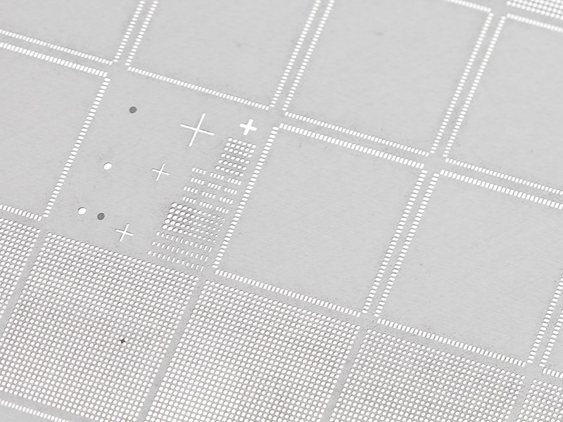
Laser-cut precision stencils such as SMD stencils are the standard for the precise application of solder and printing pastes, adhesives and other materials to rigid or flexible printed circuit boards as well as to surfaces such as silicon wafers (wafer bumping), glass or ceramic substrates (LTCC). These stencils enable precise placement and volume definition, which is crucial for the subsequent automated assembly of electronic components such as microchips, SMD components, contact elements and other semiconductor components. This technology is also used in flip-chip assembly.

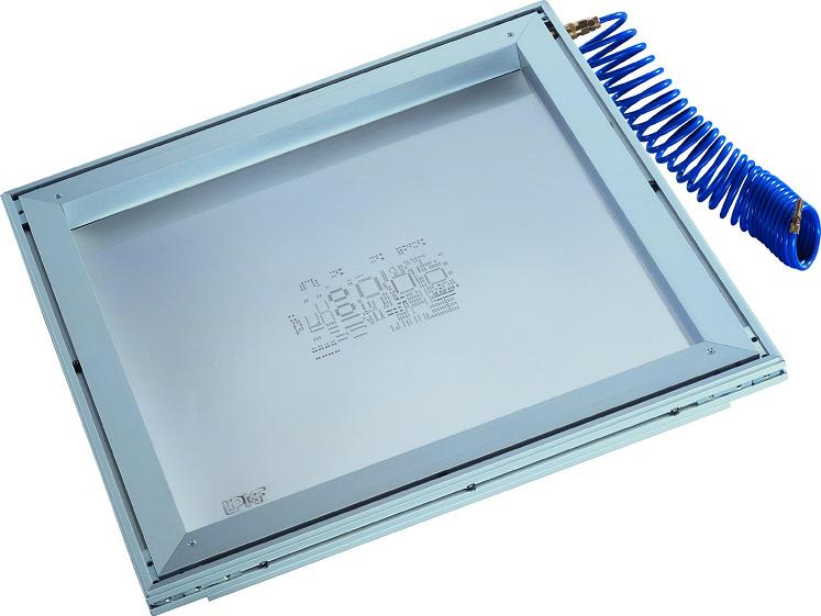
Our precision stencils are available in all standard formats and for all quick-release frames. For particularly demanding applications, we also offer electropolishing in combination with nanocoating to further improve the performance and durability of the stencils.

Advantages of our precision stencils:

  • Highest precision: laser-cut stencils guarantee exact material application.
  • Versatility: Suitable for rigid and flexible PCBs and various substrates.
  • Automated assembly: Perfect preparation for the placement and fusion of electronic components.
  • Advanced options: Electropolishing and nanocoating for demanding applications.

Opt for precision templates from KMLT® and benefit from our expertise and advanced technologies in laser cutting technology.

SMD stencils

Foto
  • Laser-cut SMD metal stencils for the industrial production of electronic assemblies

    Laser-cut SMD metal stencils are essential in the industrial production of electronic assemblies. They are used to precisely apply solder pastes or adhesives to printed circuit boards, which enables subsequent assembly with SMD components.

  • Frameless stencils with perforation for quick clamping systems

    Depending on the customer’s technical requirements, these stencils are usually manufactured as frameless sheets with perforations for quick-clamping systems. This design facilitates handling and increases efficiency in the production process.

  • Data processing

    The data processing of SMD stencils includes several important steps to ensure that the stencils can be used accurately and efficiently for solder paste printing. Here are some examples that we take into account during data processing:

    • Layout analysis: reviewing the pad layout, examining for optimization opportunities in pad shape and pad arrangement
    • Design rules: Checking for compliance with basic design rules such as the area ratio (area ratio) and aspect ratio (pad width – stencil thickness ratio) for optimum material application and avoidance of printing errors such as bridging or tombstone effects
    • Multiple duplicate creation: layout duplications and insertion of fiducials
    • Material recommendation and stencil thickness: Selection of the correct sheet thickness according to the specific requirements of the components and the layout – recommendations for special materials if necessary
  • Quality inspection of SMD stencils

    Before delivery, each SMD stencil is subjected to an optical quality check on a scanner. This enables us to guarantee maximum precision and quality in order to meet the requirements of modern electronics production.

Specil design: XXL-Stencils

SMD stencils in the VectorGuard™ format

VectorGuard™ stencils: Stainless steel 1.4301 and FineGrain material for maximum precision

In addition to stencil sheets made from 1.4301 stainless steel, we now also offer VectorGuard™ stencils made from the innovative FineGrain material. This stainless steel sheet with a particularly fine grain is a cost-effective alternative to nickel and enables smoother inner pad walls during laser cutting. The aim is to further improve the release behavior of pastes.

Advantages of FineGrain materials

  • Fine grains: FineGrain material provides a smooth and uniform surface that is ideal for precise printing.
  • Cost-effective alternative: FineGrain stainless steel is an economical solution compared to nickel, without compromising on quality.
  • Improved paste release: The smoother inner pad walls ensure optimized paste release and increase transfer efficiency.
  • Ideal for high-density applications: Particularly suitable for demanding applications that require maximum precision and reliability.

Applications

VectorGuard™ stencils made of FineGrain material are particularly interesting for high-density applications in electronics production where maximum precision and efficiency are required.

License-free perforations for quick-clamping systems

Electropolishing of SMD stencils

  • Electropolishing to optimize the inner pad edges

    During electropolishing, the surface of an anodized workpiece is abraded under the influence of direct current and electrolyte, particularly on tips and edges. This process leads to a leveling of the micro-roughness and the finest deburring, while passivity and corrosion resistance are retained.

  • KMLT® recommends electropolishing for SMD stencils

    For demanding SMD stencils, KMLT® also recommends electropolishing for surface optimization. Electropolishing minimizes the roughness within the pad walls, which significantly improves the release of the solder paste.

  • Advantages of electropolishing

    • Extremely smooth and burr-free surfaces: Electropolished stencils can be cleaned better at significantly increased intervals.
    • Improved solder paste release: Minimized roughness within the pad walls optimizes the production process.

    Further information on electropolishing can be found under surface treatment.

Nano-coating for precision stencils

  • Optimization by Aculon® NanoClear® layer

    For precision stencils, it is possible to seal the surface with an Aculon® NanoClear® coating. This nano-coating ensures that solder paste residues adhere less strongly to the pads or no longer adhere at all. This makes the stencil even easier and quicker to clean.

  • Advantages of nanocoating

    • Easy cleaning: The optimized stencil is much easier to clean.
    • Durability: This type of treatment is usually sufficient for several tens of thousands of printing processes.
    • Repeatability: The nano-coating can be repeated at any time if required.

    Take advantage of KMLT® nano-coating to maximize the efficiency and longevity of your precision stencils.